



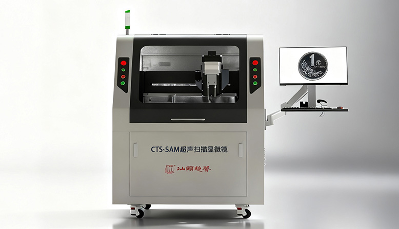


The newly launched CTS-SAM Scanning Acoustic Microscope by our STNDT is specifically designed for high-end sectors such as semiconductor manufacturing and precision component processing. It effectively meets the stringent requirements for the rapid, precise, and high-volume detection of microscopic defects.


The continuous advancement of high-end manufacturing towards greater precision, higher integration, and superior reliability has imposed unprecedented demands on the non-destructive testing (NDT) of subtle internal structures and defects in critical materials. With its non-destructive nature, deep penetration capabilities, and excellent internal imaging, the industrial Scanning Acoustic Microscope (SAM) has become a core technology for microscopic quality assessment and defect detection.
The newly launched CTS-SAM Scanning Acoustic Microscope by our STNDT is specifically designed for high-end sectors such as semiconductor manufacturing and precision component processing. It effectively meets the stringent requirements for the rapid, precise, and high-volume detection of microscopic defects.
System Composition:
The system comprises a frame, a high-precision linear motor scanning platform, a multi-degree-of-freedom probe fixture, a water tank, a water filtration and circulation system, a high-frequency pulser/receiver, a remote pulser, a high-frequency data acquisition card, an electronic control system, and software.
Domestic Core Technology:
The excitation utilizes our independently developed high-frequency pulser/receiver, the CTS-8072PR-500M. This breaks the monopoly of foreign technologies, achieving full localization and autonomous control.
Rich Scan Planning Functions:
It supports multi-workpiece planning, multi-scan surface planning, automatic path planning, teach path planning, and external path planning to meet diverse application needs.
Motion Control Functions:
Includes single-axis jog mode, single-axis absolute mode, single-axis relative mode, TCP control mode, and motion system calibration.
Comprehensive Scanning Functions:
Covers Amplitude C-scan, Depth C-scan, Multi-layer C-scan, and Through-transmission C-scan. It also features an interface wave tracking function to achieve interface wave acoustic path compensation.
C-scan Navigation:
Users can click on a specific pixel in the C-scan image to precisely move the probe to the corresponding position on the actual workpiece.
Multi-dimensional View Display:
Supports A-scan, B-scan, C-scan, D-scan, 3D views, and FFT spectrum analysis. It records A-scan waveform data and saves all views throughout the entire process.
Comprehensive and Powerful Data Analysis:
Features include:
X, Y, Z Thickness and Distance Measurement: Calculates the defect percentage based on manually drawn outlines (circle, rectangle, polygon).
CAD Template Matching: Calculates the defect percentage based on imported CAD outline templates.
Auto-defect Detection: Automatically identifies and outlines defects.
Defect Logging: Records defect lists and accurately locates defect positions.
Bonding Rate Calculation: Automatically calculates the bonding rate.
Local Gating and Thresholding: Allows users to draw a box on the C-scan image to modify local gates and thresholds.
Customizable Display: Offers multiple selectable color palettes and custom palette import. Supports scale unit switching, color scale range definition, and the display/hide functions for multiple layers.
| Item | Specification |
| Dimensions | 1364mm × 1180mm × 2050mm |
| Inspection Range | 440mm × 340mm × 200mm |
| Scanning Speed | ≤1000mm/s |
| Repeatability | X/Y Axis: ±0.001mm; Z Axis: ±0.01mm |
| Water Tank Dimensions | 876mm × 1040mm × 250mm |
| Rated Voltage | AC 220V ±5%, 50Hz ±2% |
| Rated Current | 10A |
| Power Consumption | 1.5kW |

